Electronics & Communication Gate Yearwise
Electronics and Communication Gate 2020 Questions with Answer
Ques 27 GATE 2020
For the components in the sequential circuit shown below, tpd is the propagation delay, tsetup is the setup time, and thold is the hold time. The maximum clock frequency (rounded off to the nearest integer), at which the given circuit can operate reliably, is _______ MHz.

Ques 28 GATE 2020
The impedances Z=jX for all X in the range (-∞,∞), map to the Smith chart as
Ques 29 GATE 2020
A transmission line of length 3λ/4 and having a characteristic impedance of 50 Ω is terminated with a load of 400 Ω. The impedance (rounded off to two decimal places) seen at the input end of the transmission line is _______ Ω.
Ques 30 GATE 2020
For an infinitesimally small dipole in free space, the electric field Eθ in the far field is proportional to (e⁻jkr/r)sinθ, where k=2π/λ. A vertical infinitesimally small electric dipole (δl≪λ) is placed at a distance h (h>0) above an infinite ideal conducting plane, as shown in the figure. The minimum value of h, for which one of the maxima in the far field radiation pattern occurs at θ=60°, is

Ques 31 GATE 2020
The magnetic field of a uniform plane wave in vacuum is given by
H→(x,y,z,t)=(âx+2ây+bâz)cos(ωt+3x-y-z).
The value of b is
Ques 32 GATE 2020
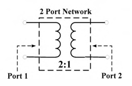
For a 2-port network consisting of an ideal lossless transformer, the parameter S₂₁ (rounded off to two decimal places) for a reference impedance of 10 Ω, is
Ques 33 GATE 2020
A single crystal intrinsic semiconductor is at a temperature of 300 K with effective density of states for holes twice that of electrons.
The thermal voltage is 26 mV.
The intrinsic Fermi level is shifted from mid-bandgap energy level by
Ques 34 GATE 2020
Consider the recombination process via bulk traps in a forward biased pn homojunction diode. The maximum recombination rate is Umax. If the electron and the hole capture cross-sections are equal, which one of the following is FALSE?
Ques 35 GATE 2020
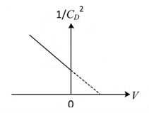
A one-sided abrupt pn junction diode has a depletion capacitance CD of 50 pF at a reverse bias of 0.2 V. The plot of 1/CD² versus the applied voltage V for this diode is a straight line as shown in the figure below. The slope of the plot is _______ ×10²⁰F⁻²V⁻¹.
Ques 36 GATE 2020
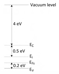
The band diagram of a p-type semiconductor with a band-gap of 1 eV is shown. Using this semiconductor, a MOS capacitor having VTH of -0.16 V, Cox' of 100 nF/cm² and a metal work function of 3.87 eV is fabricated. There is no charge within the oxide. If the voltage across the capacitor is VTH, the magnitude of depletion charge per unit area (in C/cm²) is
Ques 37 GATE 2020
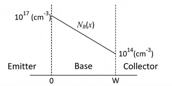
The base of an npn BJT T1 has a linear doping profile NB(x) as shown below. The base of another npn BJT T2 has a uniform doping NB of 10¹⁷ cm⁻³. All other parameters are identical for both the devices. Assuming that the hole density profile is the same as that of doping, the common-emitter current gain of T2 is
Ques 38 GATE 2020
A pn junction solar cell of area 1.0 cm² illuminated uniformly with 100 mW cm⁻², has the following parameters: Efficiency = 15% open circuit voltage = 0.7 V fill factor = 0.8, and thickness = 200 µm. The charge of an electron is 1.6×10⁻¹⁹ C. The average optical generation rate (in cm⁻³s⁻¹) is
Ques 39 GATE 2020
If V₁,V₂,...,V₆ are six vectors in R⁴ which one of the following statements is FALSE?

Total Unique Visitors