Electronics & Communication Gate Yearwise
Electronics and Communication Gate 2015 Set-1 Questions with Answer
Ques 1 GATE 2015 SET-1
A lead compensator network includes a parallel combination of R and C in the feed-forward path. If the transfer function of the compensator is Gc(s) = (s+2)/(s+4), the value of RC is
Ques 2 GATE 2015 SET-1
The open-loop transfer function of a plant in a unity feedback configuration is given as G(s) = K(s+4)/(s2(s+8)). The value of the gain K(>0) for which −1+j2 lies on the root locus is
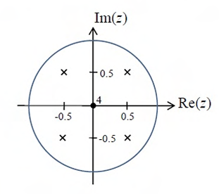
Ques 3 GATE 2015 SET-1
The pole-zero diagram of a causal and stable discrete-time system is shown in the figure. The zero at the origin has multiplicity 4. The impulse response of the system is h[n]. If h[0] = 1, we can conclude
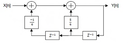
Ques 4 GATE 2015 SET-1
For the discrete-time system shown in the figure, the poles of the system transfer function are located at
Ques 5 GATE 2015 SET-1
Two sequences [a, b, c] and [A, B, C] are related as,


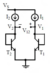
Ques 6 GATE 2015 SET-1
In the circuit shown, I1 = 80 mA and I2 = 4 mA. Transistors T1 and T2 are identical. Assume that the thermal voltage VT is 26 mV at 27°C. At 50°C, the value of the voltage V12 = (V1 − V2) in mV is
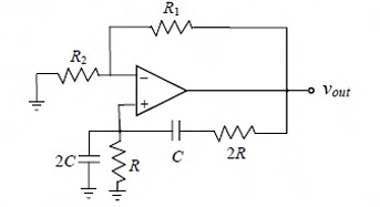
Ques 7 GATE 2015 SET-1
The circuit shown in the figure has an ideal op-amp. The oscillation frequency and the condition to sustain the oscillations, respectively, are
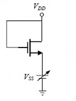
Ques 8 GATE 2015 SET-1
For the NMOSFET in the circuit shown, the threshold voltage is Vth, where Vth > 0. The source voltage VSS is varied from 0 to VDD. Neglecting the channel length modulation, the drain current ID as a function of VSS is represented by
Ques 9 GATE 2015 SET-1
A 3-input majority gate is defined by the logic function M(a,b,c) = ab + bc + ca. Which one of the following gates is represented by the function [M(M(a,b,c),M(a,b,¬c),c)]?
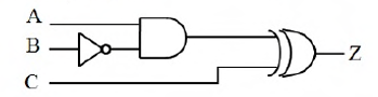
Ques 10 GATE 2015 SET-1
All the logic gates shown in the figure have a propagation delay of 20 ns. Let A = C = 0 and B = 1 until time t = 0. At t = 0, all the inputs flip (i.e. A = C = 1 and B = 0) and remain in that state. For t > 0, output Z = 1 for a duration (in ns) of
Ques 11 GATE 2015 SET-1
A MOSFET in saturation has a drain current of 1 mA for VDS = 0.5 V. If the channel length modulation coefficient is 0.05 V−1, the output resistance (in kΩ) of the MOSFET is
Ques 12 GATE 2015 SET-1
For a silicon diode with long P and N regions, the acceptor and donor impurity concentrations are 1 × 1017 cm−3 and 1 × 1015 cm−3, respectively. The lifetimes of electrons in the P region and holes in the N region are both 100 μs. The electron and hole diffusion coefficients are 49 cm2/s and 36 cm2/s, respectively. Assume kT/q = 26 mV, the intrinsic carrier concentration is 1 × 1010 cm−3, and q = 1.6 × 10⁻¹⁹ C. When a forward voltage of 208 mV is applied across the diode, the hole current density (in nA/cm2) injected from P region to N region is
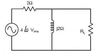
Ques 13 GATE 2015 SET-1
In the given circuit, the maximum power (in Watts) that can be transferred to the load resistor RL is

Total Unique Visitors