Electronics & Communication Gate Yearwise
Electronics and Communication Gate 2023 Questions with Answer
Ques 1 GATE 2023
A cascade of common-source amplifiers in a unity gain feedback configuration oscillates when
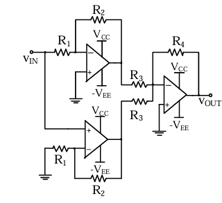
Ques 2 GATE 2023
The VOUT/VIN of the circuit shown below is
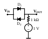
Ques 3 GATE 2023
In the circuit shown below, D1 and D2 are silicon diodes with cut-in voltage of 0.7 V. VIN and VOUT are input and output voltages in volts. The transfer characteristic is
Ques 4 GATE 2023
Let a frequency modulated (FM) signal
x(t) = A cos(ωct + kf ∫t-∞m(λ)dλ) where m(t) is a message signal of bandwidth W. It is passed through a non-linear system with output y(t) = 2x(t) + 5(x(t))2. Let BT denote the FM bandwidth. The minimum value of ωc required to recover x(t) from y(t) is
Ques 5 GATE 2023
The open loop transfer function of a unity negative feedback system is G(s) = k/s(1 + sT1)(1 + sT2). where k, T1 and T2 are positive constants. The phase cross-over frequency, in rad/s, is
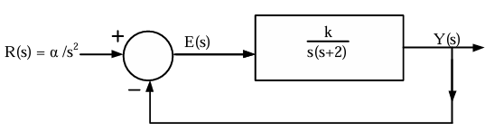
Ques 6 GATE 2023
A closed loop system is shown in the figure where k>0 and α>0. The steady state error due to a ramp input (R(s) = α/s2) is given by
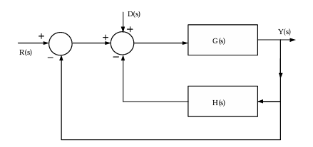
Ques 7 GATE 2023
In the following block diagram, R(s) and D(s) are two inputs. The output Y(s) is expressed as Y(s) = G1(s)R(s) + G2(s)D(s). G1(s) and G2(s) are given by
Ques 8 GATE 2023
The state equation of a second order system is
x(t) = Ax(t), x(0) is the initial condition.
Suppose λ1 and λ2 are two distinct eigenvalues of A and v1 and v2 are the corresponding eigenvectors. For constants α1 and α2, the solution, x(t), of the state equation is
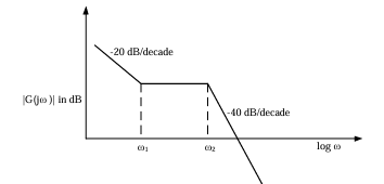
Ques 9 GATE 2023
The asymptotic magnitude Bode plot of a minimum phase system is shown in the figure. The transfer function of the system is H(s) = k(s + z)a/sb(s + p)c where k, z, p, a, b, c are positive constants. The value of (a + b + c) is ____ (rounded off to the nearest integer).
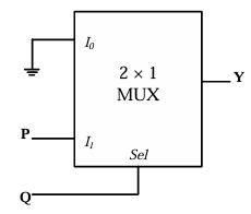
Ques 10 GATE 2023
In the circuit shown below, P and Q are the inputs. The logical function realized by the circuit shown below is
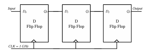
Ques 11 GATE 2023
The synchronous sequential circuit shown below works at a clock frequency of 1 GHz. The throughput, in Mbits/s, and the latency, in ns, respectively, are
Ques 12 GATE 2023
For the circuit shown below, the propagation delay of each NAND gate is 1 ns. The critical path delay, in ns, is ____ (rounded off to the nearest integer).
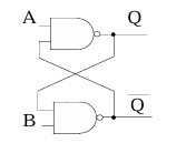
The answer to this question is 3 ns.
To understand why, let"s first recall what "critical path delay" means in a digital circuit. It is simply the longest delay path from any input to any output - the path that takes the most time for a signal to travel through, and it is this path that limits how fast the whole circuit can operate.
In this circuit, multiple NAND gates are connected together, and each one has a propagation delay of 1 ns. Now, not every input-to-output path goes through the same number of gates. Some signals might pass through just one or two gates, while others have to travel through more. The critical path is the one where the signal has to pass through the maximum number of gates.
Looking at the given circuit carefully, the longest path from input to output passes through 3 NAND gates in series. Since each gate contributes a delay of 1 ns, the total critical path delay is:
Critical Path Delay = 3 × 1 ns = 3 ns
The other paths in the circuit are shorter - they pass through fewer gates - so their delays are less than 3 ns. Only the longest chain matters when determining the critical path, and here that longest chain has exactly 3 gates.
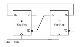
Ques 13 GATE 2023
In a given sequential circuit, initial states are Q1 = 1 and Q2 = 0. For a clock frequency of 1 MHz, the frequency of signal Q2 in kHz, is ____ (rounded off to the nearest integer).

Total Unique Visitors