Electronics & Communication Gate Yearwise
Electronics and Communication Gate 2019 Questions with Answer
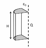
Ques 14 GATE 2019
What is the electric flux (∫E·da) through a quarter-cylinder of height H (as shown in the figure) due to an infinitely long line charge along the axis of the cylinder with a charge density of Q?
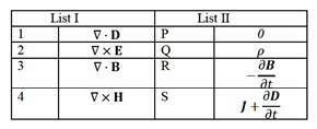
Ques 15 GATE 2019
In the table shown, List I and List II, respectively, contain terms appearing on the left-hand side and the right-hand side of Maxwell's equations (in their standard form). Match the left-hand side with the corresponding right-hand side.
Ques 16 GATE 2019
Radiation resistance of a small dipole current element of length l at a frequency of 3 GHz is 3 ohms. If the length is changed by 1%, then the percentage change in the radiation resistance, rounded off to two decimal places, is... %.
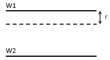
Ques 17 GATE 2019
Two identical copper wires W1 and W2, placed in parallel as shown in the figure, carry currents I and 2I, respectively, in opposite directions. If the two wires are separated by a distance of 4r, then the magnitude of the magnetic field B between the wires at a distance r from W1 is
Ques 18 GATE 2019
The dispersion equation of a waveguide, which relates the wavenumber k to the frequency (ω), is k(ω)=(1/c)√(ω2-ω02) where the speed of light c=3×10⁸ m/s and ω0 is a constant. If the group velocity is 2×10⁸ m/s, then the phase velocity is
Ques 19 GATE 2019
A rectangular waveguide of width w and height h has cut-off frequencies for TE10 and TE11 modes in the ratio 1: 2. The aspect ratio w/h, rounded off to two decimal places, is
Ques 20 GATE 2019
A standard CMOS inverter is designed with equal rise and fall times (βn=βp). If the width of the pMOS transistor in the inverter is increased, what would be the effect on the LOW noise margin (NML) and the HIGH noise margin NMH?
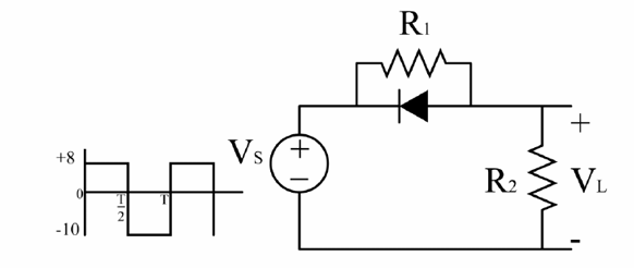
Ques 21 GATE 2019
In the circuit shown, Vs is a square wave of period T with maximum and minimum values of 8 V and -10 V, respectively. Assume that the diode is ideal and R1=R2=50 Ω. The average value of VL is... volts (rounded off to 1 decimal place).
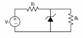
Ques 22 GATE 2019
In the circuit shown, the breakdown voltage and the maximum current of the Zener diode are 20 V and 60 mA, respectively. The values of R1 and RL are 200 Ω and 1 kΩ, respectively. What is the range of Vi that will maintain the Zener diode in the 'on' state?
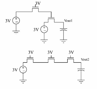
Ques 23 GATE 2019
In the circuits shown, the threshold voltage of each nMOS transistor is 0.6 V. Ignoring the effect of channel length modulation and body bias, the values of Vout1 and Vout2, respectively, in volts, are
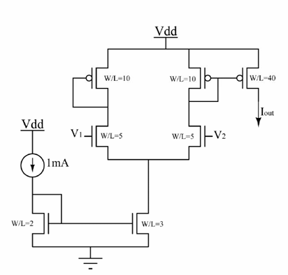
Ques 24 GATE 2019
In the circuit shown, V1=0 and V2=Vdd. The other relevant parameters are mentioned in the figure. Ignoring the effect of channel length modulation and the body effect, the value of Iout is... mA (rounded off to 1 decimal place).
Ques 25 GATE 2019
In the circuit shown, the threshold voltages of the PMOS (|Vtp|) and nMOS (Vtn) transistors are both equal to 1 V. All the transistors have the same output resistance rds of 6 MΩ. The other parameters are listed below: μnCox=60 μA/V2; (w/L)nMOS=5 and μpCox=30 μA/V2; (w/L)PMOS=10. μn and μp are the carrier mobilities, and Cox is the oxide capacitance per unit area. Ignoring the effect of channel length modulation and body bias, the gain of the circuit is... (rounded off to 1 decimal place).
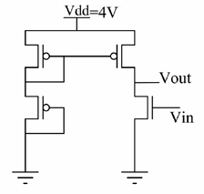
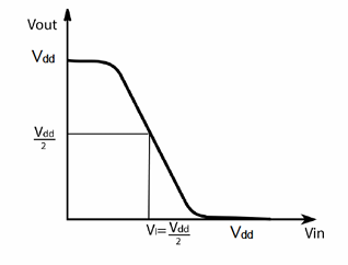
Ques 26 GATE 2019
A CMOS inverter, designed to have a mid-point voltage Vi equal to half of Vdd, as shown in the figure, has the following parameters: Vdd=3 V, μnCox=100μA/V2; Vtn=0.7 V for nMOS, μpCox=40μA/V2; |Vtp|=0.9 V for pMOS. The ratio of (W/L)n to (W/L)p is equal to... (rounded off to 3 decimal places).

Total Unique Visitors