Electronics & Communication Gate Yearwise
Electronics and Communication Gate 2013 Set-2 Questions with Answer
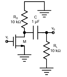
Ques 1 Gate 2013 SET-2
The ac schematic of an NMOS common-source stage is shown in the figure below, where part of the biasing circuits has been omitted for simplicity. For the n-channel MOSFET M, the transconductance gm = 1 mA/V, and body effect and channel length modulation effect are to be neglected. The lower cutoff frequency in Hz of the circuit is approximately at
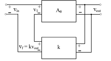
Ques 2 GATE 2013 SET-2
In a voltage-voltage feedback as shown below, which one of the following statements is TRUE if the gain k is increased?
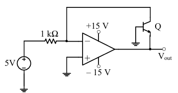
Ques 3 Gate 2013 SET-2
In the circuit shown below what is the output voltage (Vout) if a silicon transistor Q and an ideal op-amp are used?
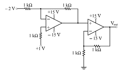
Ques 4 Gate 2013 SET-2
In the circuit shown below the op-amps are ideal. Then Vout in Volts is
Ques 5 Gate 2013 SET-2
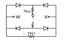
A voltage 1000 sin ωt Volts is applied across YZ. Assuming ideal diodes, the voltage measured across WX in Volts, is
Ques 6 Gate 2013 SET-2
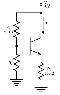
In the circuit shown below, the silicon npn transistor Q has a very high value of β. The required value of R2 in kΩ to produce IC = 1 mA is
Ques 7 Gate 2013 SET-2
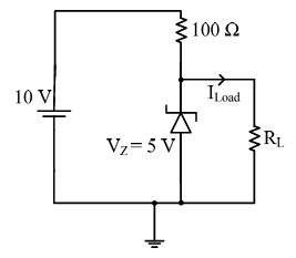
In the circuit shown below, the knee current of the ideal Zener diode is 10 mA. To maintain 5 V across RL, the minimum value of RL in Ω and the minimum power rating of the Zener diode in mW, respectively, are
Ques 8 Gate 2013 SET-2
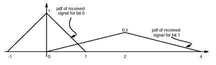
Bits 1 and 0 are transmitted with equal probability. At the receiver, the pdf of the respective received signals for both bits are as shown below. If the detection threshold is 1, the BER will be
Ques 9 Gate 2013 SET-2
Bits 1 and 0 are transmitted with equal probability. At the receiver, the pdf of the respective received signals for both bits are as shown below.
Ques 10 Gate 2013 SET-2
The bit rate of a digital communication system is R kbits/s. The modulation used is 32-QAM. The minimum bandwidth required for ISI free transmission is
Ques 11 Gate 2013 SET-2
The state diagram of a system is shown below. A system is described by the state-variable equations Ẋ = AX + Bu; y = CX + Du.
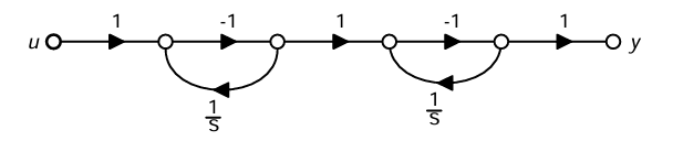
Ques 12 Gate 2013 SET-2
The state transition matrix eAt of the system shown in the figure above is
Ques 13 Gate 2013 SET-2
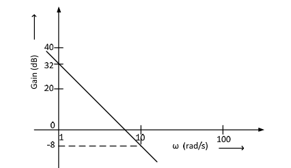
The Bode plot of a transfer function G(s) is shown in the figure below. The gain 20log|G(s)| is 32 dB and -8 dB at 1 rad/s and 10 rad/s respectively.

Total Unique Visitors