Electronics & Communication Gate Yearwise
Electronics and Communication Gate 2017 Set-2 Questions with Answer
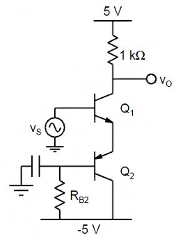
Ques 27 GATE 2017 SET-2
In the circuit shown, transistors Q1 and Q2 are biased at a collector current of 2.6 mA. Assuming that transistor current gains are sufficiently large to assume collector current equal to emitter current and thermal voltage of 26 mV, the magnitude of voltage gain Vo/VS in the mid-band frequency range is (up to second decimal place).
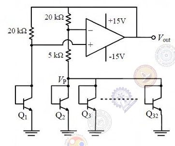
Ques 28 GATE 2017 SET-2
In the voltage reference circuit shown in the figure, the op-amp is ideal and the transistors Q1, Q2,...,Q32 are identical in all respects and have infinitely large values of common-emitter current gain (β). The collector current (IC) of the transistors is related to their base-emitter voltage (VBE) by the relation IC=ISexp(VBE/VT). Where IS is the saturation current. Assume that the voltage Vp shown in the figure is 0.7 V and the thermal voltage VT=26 mV.
Ques 29 GATE 2017 SET-2
An n-channel enhancement mode MOSFET is biased at VGS>VTH and VDS>(VGS-VTH). where VGS is the gate-to-source voltage, VDS is the drain-to-source voltage and VTH is the threshold voltage. Considering channel length modulation effect to be significant, the MOSFET behaves as a
Ques 30 GATE 2017 SET-2
An npn bipolar junction transistor (BJT) is operating in the active region. If the reverse bias across the base-collector junction is increased, then
Ques 31 GATE 2017 SET-2
Consider an n-channel MOSFET having width W. length L. electron mobility in the channel μn and oxide capacitance per unit area Cox. If gate-to-source voltage VGS=0.7 V, drain-to-source voltage VDS=0.1 V, (μnCox)=100 μA/V2, threshold voltage VTH=0.3 V and (W/L)=50, then the transconductance gm (in mA/V) is
Ques 32 GATE 2017 SET-2
A MOS capacitor is fabricated on p-type Si (Silicon) where the metal work function is 4.1 eV and electron affinity of Si is 4.0 eV. EC-EF=0.9 eV, where EC and EF are the conduction band minimum and the Fermi energy levels of Si, respectively. Oxide εr=3.9. εo=8.85×10⁻¹⁴F/cm, oxide thickness tox=0.1 μm and electronic charge q=1.6×10⁻¹⁹ C. If the measured flat band voltage of this capacitor is -1 V. then the magnitude of the fixed charge at the oxide-semiconductor interface, in nC/cm2 is
Ques 33 GATE 2017 SET-2
For a particular intensity of incident light on a silicon pn junction solar cell, the photocurrent density (JL) is 2.5 mA/cm2 and the open-circuit voltage (Voc) is 0.451 V. Consider thermal voltage (VT) to be 25 mV. If the intensity of the incident light is increased by 20 times, assuming that the temperature remains unchanged, Voc (in volts) will be
Ques 34 GATE 2017 SET-2
Two n-channel MOSFETs. T1 and T2, are identical in all respects except that the width of T2 is double that of T1. Both the transistors are biased in the saturation region of operation, but the gate overdrive voltage (VGS-VTH) of T2 is double that of T1. where VGS and VTH are the gate-to-source voltage and threshold voltage of the transistors, respectively. If the drain current and transconductance of T1 are ID1 and gm1 respectively, the corresponding values of these two parameters for T2 are
Ques 35 GATE 2017 SET-2
An abrupt pn junction (located at x=0) is uniformly doped on both p and n sides. The width of the depletion region is W and the electric field variation in the x-direction is E(x). Which of the following figures represents the electric field profile near the pn junction?
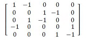
Ques 36 GATE 2017 SET-2
The rank of the matrix
Ques 37 GATE 2017 SET-2
The general solution of the differential equation d2y/dx2+2dy/dx-5y=0 in terms of arbitrary constants K1 and K2 is
Ques 38 GATE 2017 SET-2
The smaller angle (in degrees) between the planes x+y+z=1 and 2x-y+2z=0 is
Ques 39 GATE 2017 SET-2
The residues of a function f(z)=1/((z-4)(z+1)3) are

Total Unique Visitors