Electrical Engineering Gate Yearwise
Electrical Gate 2025
Electrical Gate 2024
Electrical Gate 2023
Electrical Gate 2022
Electrical Gate 2021
Electrical Gate 2020
Electrical Gate 2019
Electrical Gate 2018
Electrical Gate 2017 (Set 1)
Electrical Gate 2017 (Set 2)
Electrical Gate 2016 (Set 1)
Electrical Gate 2016 (Set 2)
Electrical Gate 2015 (Set 1)
Electrical Gate 2015 (Set 2)
Electrical Gate 2014 (Set 1)
Electrical Gate 2014 (Set 2)
Electrical Gate 2014 (Set 3)
Electrical Gate 2013 (Set 1)
Electrical Gate 2013 (Set 2)
Electrical Gate 2013 (Set 3)
Electrical Engineering Gate 2026 Questions with Answer
Ques 40 GATE 2026
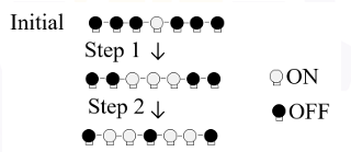
Consider a linear arrangement of seven bulbs, each of which can be in the ON or OFF states. The initial configuration of the bulbs is shown in the figure. In every Step, the states of the bulbs are changed based on the following rules:
• Any OFF bulb with exactly one ON neighbor at the end of the previous Step is turned ON.
• Any ON bulb with both neighbors ON at the end of the previous Step is turned OFF.
• The state of any bulb not meeting the conditions above is left unchanged.
The state of bulbs at the end of Step 1 and Step 2 are also shown in the figure.
The number of bulbs which are ON at the end of Step 8 is ______
Ques 41 GATE 2026
P and Q are two positive integers such that P2 = Q2 + 13.
The product of the numbers P and Q is _________
Ques 42 GATE 2026
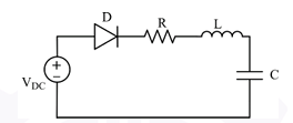
A circuit with ideal elements is shown (diode D, resistor R, inductor L, capacitor C in series with DC source).
Ques 43 GATE 2026
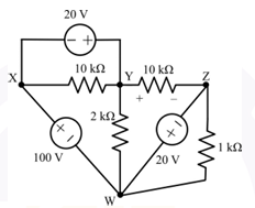
For the circuit shown, which one of the following options correctly identifies the Thevenin’s equivalent parameters between nodes Y and Z?
Ques 44 GATE 2026
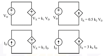
Refer to the four circuits shown,
Ques 45 GATE 2026
A single-phase voltage source vs = 325 sin(2π50t) V delivers a current, i = 12 sin(2π50t) + 9 sin(2π150t) A to a load.
The load power factor, correct up to two decimal places, is:
Ques 46 GATE 2026
An electrical component has voltage drop v = Vmsin(ωt), when the current through it is i = Imsin(ωt − θ).
What is the average power dissipated over a half cycle corresponding to ω?
Ques 47 GATE 2026
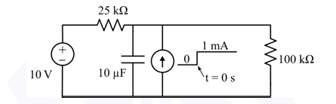
The electrical network shown has an independent voltage source (10 V) and a current source (1 u(t) mA).
The voltage across the capacitor at time instants (in seconds) t = 0+, t = 0.50, and t = ∞, respectively, is:
Ques 48 GATE 2026
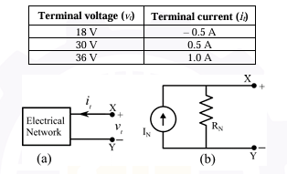
The terminal voltage and current of a linear electrical network shown in Figure (a) are given in the table.
Ques 49 GATE 2026
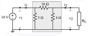
Consider the two-port network shown. For maximum power transfer to the resistive load (RL), the value of RL should be__________ Ω
Ques 50 GATE 2026
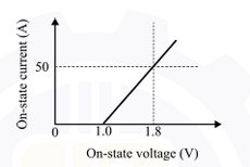
The figure shows a straight-line approximation for the forward characteristics of a power diode. A continuous on-state current of 15 A is flowing through the diode.
Ques 51 GATE 2026
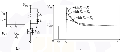
Consider the circuit shown in Figure (a). A gate pulse vg is applied between time instants t0 and t1. After t1, during the MOSFET turn OFF process, it experiences a voltage overshoot.
Based on the vds waveforms shown in Figure (b), which one of the following options is correct?
Ques 52 GATE 2026
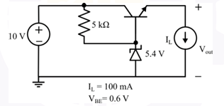
In the linear regulator circuit shown, the base to emitter voltage VBE of the BJT is 0.6 V. The Zener diode clamps the base voltage to 5.4 V. Ignore the biasing current of the Zener diode and BJT.
The maximum possible efficiency of the regulator circuit is ___________ %
(Round off to one decimal place)

Total Unique Visitors