Electrical Engineering Gate Yearwise
Electrical Gate 2024
Electrical Gate 2023
Electrical Gate 2022
Electrical Gate 2021
Electrical Gate 2020
Electrical Gate 2019
Electrical Gate 2018
Electrical Gate 2017 (Set 1)
Electrical Gate 2017 (Set 2)
Electrical Gate 2016 (Set 1)
Electrical Gate 2016 (Set 2)
Electrical Gate 2015 (Set 1)
Electrical Gate 2015 (Set 2)
Electrical Gate 2014 (Set 1)
Electrical Gate 2014 (Set 2)
Electrical Gate 2014 (Set 3)
Electrical Gate 2013 (Set 1)
Electrical Gate 2013 (Set 2)
Electrical Gate 2013 (Set 3)
Electrical Engineering Gate 2023 Questions with Answer
Ques 1 GATE 2023
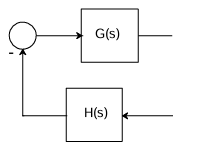
For the block diagram shown in the figure, the transfer function Y(s)/R(s) is _______.

Ques 2 GATE 2023
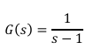
In the Nyquist plot of the open-loop transfer function G(s)H(s)=(3s+5)/(s-1) corresponding to the feedback loop shown in the figure, the infinite semi-circular arc of the Nyquist contour in s-plane is mapped into a point at _______.
Ques 3 GATE 2023
Consider a unity-gain negative feedback system consisting of the plant G(s) and a proportional-integral controller. Let the proportional gain and integral gain be 3 and 1, respectively. For a unit step reference input, the final values of the controller output and the plant output, respectively, are
Ques 4 GATE 2023
The magnitude and phase plots of an LTI system are shown in the figure. The transfer function of the system is _______.

Ques 5 GATE 2023
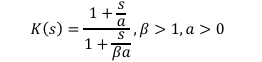
Consider a lead compensator of the form
Ques 6 GATE 2023
Consider the state-space description of an LTI system with matrices

Ques 7 GATE 2023
Neglecting the delays due to the logic gates in the circuit shown in the figure, the decimal equivalent of the binary sequence [ABCD] of initial logic states, which will not change with the clock, is _______.

Ques 8 GATE 2023
In the figure, the electric field E and the magnetic field B point to x and z directions, respectively, and have constant magnitudes. A positive charge 'q' is released from rest at the origin. Which of the following statement(s) is/are true?

Ques 9 GATE 2023
An infinite surface of linear current density K=5âx A/m exists on the x-y plane, as shown in the figure. The magnitude of the magnetic field intensity (H) at a point (1,1,1) due to the surface current in Ampere/meter is _______. (Round off to 2 decimal places).

Ques 10 GATE 2023
Consider the OP AMP based circuit shown in the figure. Ignore the conduction drops of diodes D1 and D2. All the components are ideal and the breakdown voltage of the Zener is 5 V. Which of the following statements is true?

Ques 11 GATE 2023
An 8-bit ADC converts analog voltage in the range of 0 to +5 V to the corresponding digital code as per the conversion characteristics shown in the figure. For Vin=1.9922 V, which of the following digital output, given in hex, is true?

Ques 12 GATE 2023
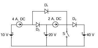
All the elements in the circuit shown in the following figure are ideal. Which of the following statements is/are true?
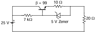
Ques 13 GATE 2023
The Zener diode in the circuit has a breakdown voltage of 5 V. The current gain β of the transistor in the active region is 99. Ignore base-emitter voltage drop VBE. The current through the 20 Ω resistance in milliamperes is _______. (Round off to 2 decimal places).

Total Unique Visitors