EC > GATE 2020 > BJT
The base of an npn BJT T1 has a linear doping profile NB(x) as shown below. The base of another npn BJT T2 has a uniform doping NB of 10¹⁷ cm⁻³. All other parameters are identical for both the devices. Assuming that the hole density profile is the same as that of doping, the common-emitter current gain of T2 is
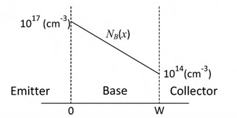
Correct : mta
Similar Questions
Which of the following statements is/are true for a BJT with respect to its DC current gain (β)?
The correct circuit representation of the structure shown in the figure is
A BJT is biased in forward active mode. Assume VBE = 0.7 V, kT/q = 25 mV and reverse saturation current IS = 10-13 A. The transconductance of the BJT (in mA/V)...

Total Unique Visitors
Loading......