EC > GATE 2017 SET-2 > PN Junction Diode
An abrupt pn junction (located at x=0) is uniformly doped on both p and n sides. The width of the depletion region is W and the electric field variation in the x-direction is E(x). Which of the following figures represents the electric field profile near the pn junction?
A
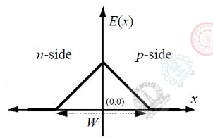
B
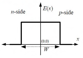
C
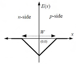
D
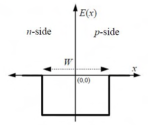
Correct : a
Similar Questions
The photocurrent of a PN junction diode solar cell is 1 mA.The voltage corresponding to its maximum power point is 0.3 V.If the thermal voltage is 30 mV, the re...
A one-sided abrupt pn junction diode has a depletion capacitance CD of 50 pF at a reverse bias of 0.2 V. The plot of 1/CD² versus the applied voltage V for this...
In an ideal pn junction with an ideality factor of 1 at T=300 K, the magnitude of the reverse-bias voltage required to reach 75% of its reverse saturation curre...

Total Unique Visitors
Loading......