EC > GATE 2017 SET-2 > Diode Circuits
In the figure. D1 is a real silicon pn junction diode with a drop of 0.7 V under forward bias condition and D2 is a Zener diode with breakdown voltage of 6.8 V. The input Vin(t) is a periodic square wave of period T, whose one period is shown in the figure.
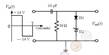 Assuming 10τ<<T, where τ is the time constant of the circuit, the maximum and minimum values of the output waveform are respectively.
Correct : a
Similar Questions
In the circuit shown, the n: 1 step-down transformer and the diodes are ideal.The diodes have no voltage drop in forward biased condition.If the input voltage (...
In the circuit shown below, D1 and D2 are silicon diodes with cut-in voltage of 0.7 V. VIN and VOUT are input and output voltages in volts. The transfer charact...
All the diodes in the circuit given below are ideal.Which of the following plots is/are correct when VI (in Volts) is swept from -M to M?

Total Unique Visitors
Loading......