EC > GATE 2015 SET-3 > Sequential Circuits
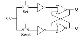
An SR latch is implemented using TTL gates as shown in the figure. The set and reset pulse inputs are provided using the push-button switches. It is observed that the circuit fails to work as desired. The SR latch can be made functional by changing
Correct : d
Similar Questions
The sequence of states $(Q_1 Q_0)$ of the given synchronous sequential circuit is
The synchronous sequential circuit shown below works at a clock frequency of 1 GHz. The throughput, in Mbits/s, and the latency, in ns, respectively, are
In a given sequential circuit, initial states are Q1 = 1 and Q2 = 0. For a clock frequency of 1 MHz, the frequency of signal Q2 in kHz, is ____ (rounded off to...

Total Unique Visitors
Loading......