EC > GATE 2014 SET-2 > PN Junction
Consider an abrupt PN junction (at T = 300 K) shown in the figure. The depletion region width Xn on the N-side of the junction is 0.2 μm and the permittivity of silicon (εsi) is 1.044×10⁻¹² F/cm. At the junction, the approximate value of the peak electric field (in kV/cm) is _________.
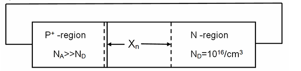
Correct : 31
Similar Questions
The doping concentrations on the p-side and n-side of a silicon diode are 1 × 1016 cm-3 and 1 × 1017 cm-3, respectively. A forward bias of 0.3 V is applied to t...
When a silicon diode having a doping concentration of NA = 9 × 1016 cm-3 on p-side and ND = 1 × 1016 cm-3 on n-side is reverse biased, the total depletion width...
The donor and accepter impurities in an abrupt junction silicon diode are 1 × 1016 cm−3 and 5 × 1018 cm−3, respectively. Assume that the intrinsic carrier conce...

Total Unique Visitors
Loading......