EC > Gate 2013 SET-2 > MOSFET
The small-signal resistance (i.e., dVB/dID) in kΩ offered by the n-channel MOSFET M shown in the figure below, at a bias point of VB = 2 V is (device data for M: device transconductance parameter kN = μnCox(W/L) = 40 μA/V2, threshold voltage VTN = 1 V, and neglect body effect and channel length modulation effects)
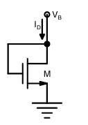
Correct : b
Similar Questions
An NMOS transistor operating in the linear region has IDS of 5 μA at VDS of 0.1 V.
Keeping VGS constant, the VDS is increased to 1.5 V.
Given that μnCox(W/L)...
Consider the CMOS circuit shown in the figure (substrates are connected to their respective sources). The gate width (W) to gate length (L) ratios (W/L) of the...
The ideal long channel nMOSFET and pMOSFET devices shown in the circuits have threshold voltages of 1 V and −1 V, respectively. The MOSFET substrates are connec...

Total Unique Visitors
Loading......